2 What is the concept of nano process? A human hair is typically 50,000-60,000 nanometers in diameter. In terms of 50,000 nanometers, 2 nanometers is equivalent to 25,000 axial sections of hair.
According to the Nihon Keizai Shimbun, the original company Rapidus was established after receiving subsidies from the Japanese government and funding from eight companies including Toyota Group and Nippon Telecom and Telephone Co., LTD. The joint venture hopes to have the capacity to produce 2-nanometer process chips by 2025-2030.
Japan is already a decade behind its rival Taiwan Semiconductor. powered by A nanometer is essentially a unit of length. Apple's familiar A16 Bionic chips and Snapdragon 8 chips are made from 4-nanometer processes.
A chip is a type of integrated circuit that integrates components such as resistors and transistors into a tiny flat plate. These electronic components are connected in series by connecting wires. With the development of technology, the lithography machine can be used to integrate the existing tens of billions of transistors on this tiny plate. The higher the integration degree, the higher computing power of the chip, the stronger the performance naturally.
Rapidus was established to acquire manufacturing technology for next-generation logic semiconductors (semiconductors for control, processing, and computational processing), establish a mass production line, and commercialize the contract manufacturing business in Japan. For Rapidus, there are a number of hurdles to overcome to achieve these goals. "Japan is 10 to 20 years behind its competitors in cutting-edge logic chips, and it is not easy to recover," said Soyuki Koike, president of the current company, at a press conference on the launch of Rapidus.
The amount of investment required for R&D and manufacturing of advanced logic semiconductors has increased to one trillion yen. Not only the costly equipment and research and development, but also the manufacturing process requires advanced technology and experience. Japanese companies failed to keep up with the investment competition in the 2010s, and logic semiconductor plants in Japan are still around 40 nanometers.
Rapidus received 7.3 billion yen in investment from eight Japanese companies, in addition to 70 billion yen from the Japanese government. The original company, which plans to start production in 2027, has already begun to secure equipment and talent.
Analysts were skeptical that the current company would be an immediate success amid fierce global competition, Kyodo News reported. The Japanese government has set aside only 70 billion yen in financial support, compared with the $52.7 billion proposed by the Chip and Science Act. Hideki Yasuda, senior analyst at Toyo Securities, said the Y70bn was "certainly not sufficient" to make the original company competitive in the global market, where the chip industry needs about Y1tn of investment a year. "It is difficult to force private companies to bear such costs, so the question is whether the Japanese government is prepared to do so."
TSMC and Samsung Electronics have mastered the technology to mass-produce 3-nanometer products and are planning to mass-produce next-generation 2-nanometer chips by 2025. In the face of competition from contract giants such as TSMC, Mr Koike said Rapidus was "not going to catch up with TSMC and Samsung in terms of scale". Rapidus will explore a different model from TSMC and Samsung, which make semiconductors for end-products such as smartphones in large quantities.
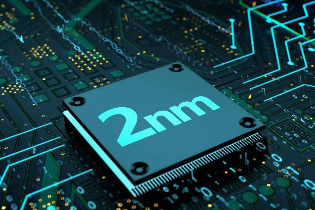
2 nanometers is a current track.
Now, in addition to TSMC and Samsung, Intel has plans to return to the top with a 2-nanometer process. Meanwhile, governments and companies in Europe and Japan are also hoping to revive chip manufacturing through 2-nanometer processes. Why have so many companies, even countries and regions, decided to bet on 2-nanometer chips?
First of all, compared with the current mainstream chips, the power consumption of 2-nanometer chips will be considerably reduced, while the performance will be considerably improved. This means that the battery life and performance of electronic products such as mobile phones and computers will be considerably improved. For the auto industry, 2-nanometer chips could speed up the speed at which self-driving cars can detect objects and shorten the computing time of autonomous driving systems.
On the other hand, according to Forbes, the process architecture, materials and equipment involved in the 2-nanometer semiconductor process will be updated. Technological innovation means that the industrial landscape is likely to be reshuffled, which is an essential reason why numerous companies have invested in this current track. According to Forbes, semiconductor processes are approaching physical limits, thus changes in transistor architecture, the use of different materials, and likely packaging technology are key factors in the development of 2-nanometer process chips. At present, although numerous countries and companies are developing 2 nanometer chips, 2 nanometer chips still face multiple bottlenecks in terms of architecture, materials and equipment.
The current focus of nano process technology is that transistor architecture will move from FinFET to GAAfet era. The current architecture can effectively control the leakage problem of 2 nm chip, and may become the mainstream architecture of 2 nm process. However, only Samsung has made significant achievements in the GAAFET architecture manufacturing process. In June, Samsung announced mass production of its Gaafet-based 3nm chip.
Secondly, the selection and application of current materials will also play a crucial role in the development of 2-nanometer processes. Specifically, two-dimensional or one-dimensional materials such as graphene, carbon nanotubes and transition metal compounds are expected to replace silicon-based materials due to their smaller sizes. In addition, the process of making 2-nanometer chips also requires the support of equipment such as lithography machines. At present, the photolithography machine that can meet the production demand of 2-nanometer process still needs to break through the innovation of optical resolution, photoresist and additional related technologies and equipment series.
At the same time, the challenge of manufacturing costs cannot be ignored. According to relevant data, the 7nm process costs at least $300 million to develop, the 5nm process costs an average of $542 million, and the 3nm and 2nm process starting price of at least $1 billion.